Transistors
- From 2300 (1971) to 21 Mil (2000) to 67 Bil (2022, M2 Max) transistors.
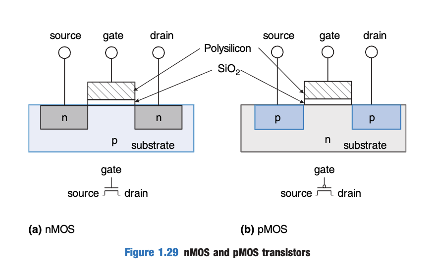
- MOS (Conductors, Insulators, Semiconductors)
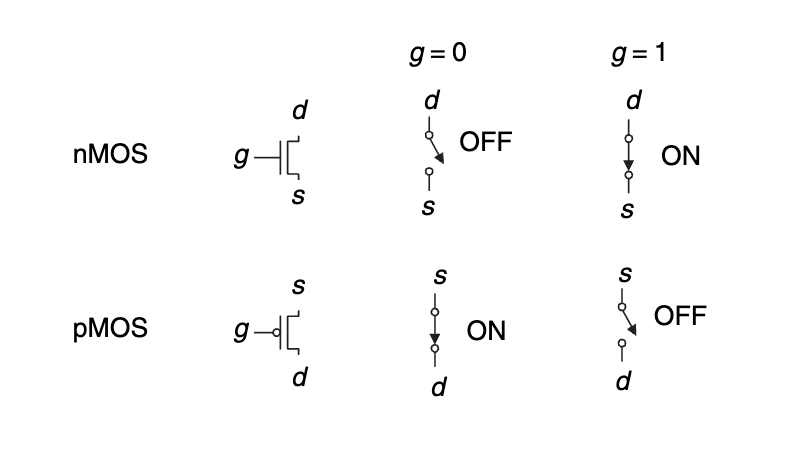
- Voltage and Type: Source and Drain get connected or not (Gate).
- Transistor as switches.
- n-type: the circuit is closed when the gate is supplied with 3V, transistor gets high voltage, the connection from source to drain is closed. 0V: circut open, light off
- p-type: the circuit is closed when the gate is supplied with 0V. marked with a dot. 0V: closed circuit, light on.
CMOS
- p-type pulls up, n-type pulls down the output (the voltage)
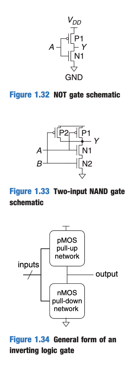
Logic Gates
Boolean Algebra
-
NOT:
-
AND:
-
OR:
-
Minterm: Product (AND) that includes all input variables of a row in the truth table exactly once (DNF). For
-
Maxterm: Sum (OR) that includes all input variables of a row in the truth table exactly once. For
-
Implicant: Product (AND) of literals ( or )
-
SOP, sum of products.
-
POS, product of sums.
-
Create the truth table → bring into SOP/POS form → boolean simplification rules
Simplification
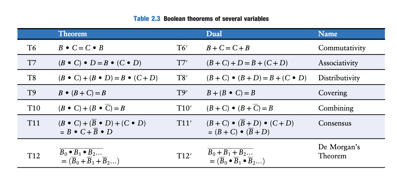
Dual
-
- to and vice versa
- 0 to 1 and vice versa
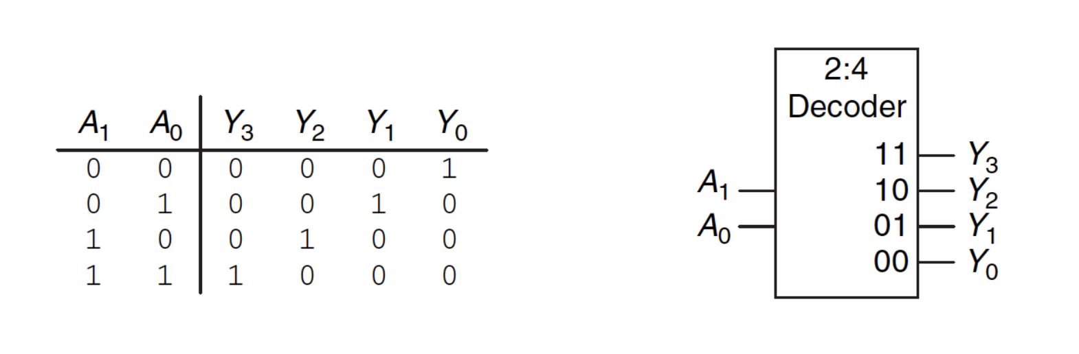
Decoder
For example 2-to-4 decoder is about choosing one ouput (Y) depending on the input and .
Exactly one output (Y) is 1 and the rest is 0.
Multiplexer (Selector)
Selects one signal from N available inputs. Needs select controls
Latency and Power Consumption
- series connections are slower than parallel connections (more resistance on the wire)
- dynamic power consumption: charge capacitance as signal change ( to or to )
- capacitance of the circuit supply voltage charging frequency of the capacitor
- voltage vs performance
- static power consumption: . Power used when signals do not change. supply voltage leakage current
- energy is integral of power. energy determines battery life
Full adder
More reading:
Adders for higher bit addition
depends on sequential adders, thus slow
PLA
A Programmable Logic Array is a customizable hardware construct used to implement specific digital logic functions, basically a super basic version of an FPGA. It is built using two distinct sets of logic gates: a column of AND gates whose outputs feed into a column of OR gates. You program the PLA by defining exactly which AND gate outputs connect to which OR gate inputs in the central connection block.
This physical AND-to-OR layout is specifically designed to calculate “Sum of Products” (SOP) equations. By connecting the right “minterms,” the PLA can implement any required N-input, M-output logic function.
Implementing a Full adder
Completeness
Success
Logically complete, meaning any trutz table (logic function) can be build only with them
- NAND
- NOR
- {AND, OR, NOT}
Example: NAND is logically complete
Definition of NAND:
Equality Checker
ALU
One component that can act as a bunch of different components.
Tri-State Buffer
A and E input, Y output.
- E=0: New Z-State is no signal, as if wire cut
- E=1: Acts as normal wire (Y=E)
Imagine a wire connecting the CPU and memory. At any time only the CPU or the memory can place a value on the wire, both not both. You can have two tri-state buffers: one driven by CPU, the other memory; and ensure at most one is enabled at any time