Glossary
| Abbreviation | Full Term | Description |
|---|---|---|
| MAR | Memory Address Register | Holds target memory address for R/W |
| MDR | Memory Data Register | Holds data being moved to/from memory |
| ALU | Arithmetic Logic Unit | Executes math and logic operations |
| I/O | Input / Output | Hardware for external interaction (e.g., keyboard) |
| IR | Instruction Register | Stores instruction currently being executed |
| PC | Program Counter | Stores address of next instruction |
| ISA | Instruction Set Architecture | Processor instruction “vocabulary” |
| LC-3 | Little Computer 3 | Architecture with 8 general-purpose registers |
| MIPS | Microprocessor without… | Architecture with 32 general-purpose registers |
| LDR | Load Register | Moves data from memory into register |
| ADD | Add(-ition) | Sums values from register file |
| OP | Opcode | Specifies operation type (e.g., ) |
| SR | Source Register | Register containing input data |
| DR | Destination Register | Register where result is stored |
| IMM | Immediate | Literal constant encoded in instruction |
| RS | Source Register | Register containing input data in MIPS |
| RT | Target Register | Destination or second source register in MIPS |
Principles
- Stored-Program: Instructions stored in linear memory array, memory between insstructions and data is unified
- Sequential Instruction Execution: Instructions executed sequentially one at the time. Program counter identifies current instruction.
Component Overview
Memory
- Stores Programs and Data through bits.
- bits is the smallest unit
- a byte is typically 8 bits
- a word consists of multiple bytes
- Each storage location is identified by its address. The set of all addresses is called address space.
- Addressability: number of bits at an address location. Could be f.ex.
- word-addressable, meaning each word has a unique address
- byte-addressable, meaning each byte has a unique address (common). A 32-bit word at address
Xwould occupy bytesX,X+1,X+2,X+3.
Example, suppose a word is 4 Bytes (4 columns in one row). That’s why the adresses on the left make 4er Schritte (C is 12). A box is 1 Byte, the content in hex format.
Accessing Memory
- MAR: Memory Address Register Holds the address of where the data is stored or where to save something.
- MDR: Memory Data Register Holds the actual data
Conventions to order the four bytes in a row:
- Big Endian: Most significant byte gets lower byte address
- Little Endian: Most significant byte gets higher byte address
Processing Unit
- ALU performs arithmetic and bitwise operations.
- Registers hold temporary data.
Registers
- Memory is large but slow, Registers are for fast access
- Computer has small memory close to ALU for fast temporary access (f.ex. for intermediate results in a calculation)
- The collection of those single registers is called the Register File.
- F.ex.
LC-3has 8 general purpose registers,MIPShas 32 - Implementation (03 Storage)
I/O, Input and Output
Well, the obvious. Here, we mainly consider keyboard and monitor.
Control Unit
Conducts step by step process of executing a program. Sends signals to ALU to select an operation, to registers to read or write data, to memory to initiate read or write cycles.
- Instruction Register: keeps track of instructions that are being processed
- Program Counter / Instruction Pointer: contains address of next instruction to process
Instructions
- an instruction is the most basic unit of computer processing
- the ISA (instruction set architecture) is like the “vocabulary” of the computer language
- can be written as machine language (0’s and 1’s) or Assembly (human readable)
LC-3vsMIPSinstructions
- Opcode: what to do
- Operands: who does it
3 Types of Instructions
- operate instructions (in the ALU)
- move data
- change sequence of execution
Assembly Instructions, Examples
Assembly:
add a, b, cLC-3 registers:
b = R1
c = R2
a = RO
MIPS-registers
b = $s1
c = $s2
a = $s0
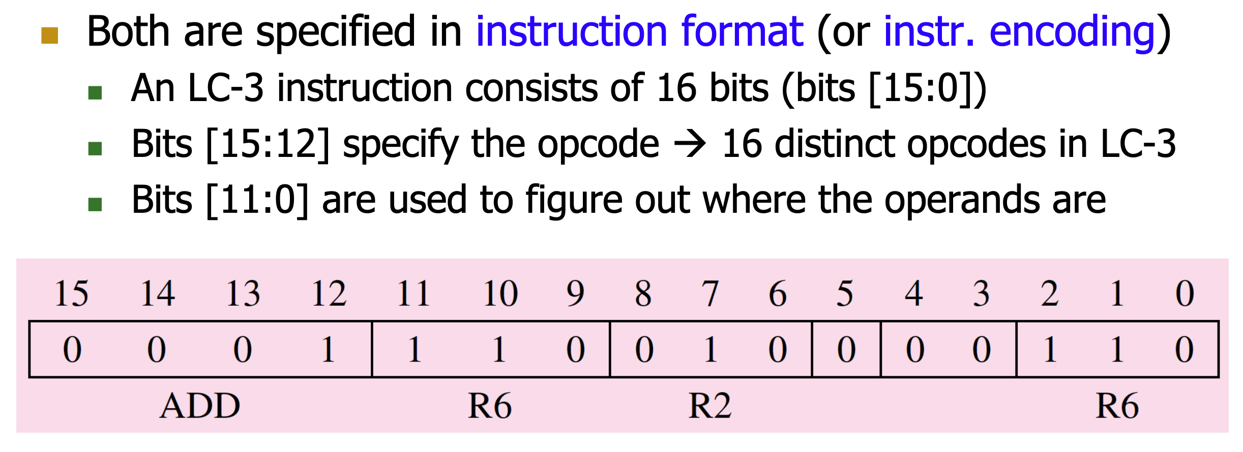
Example for an LC-3 Instruction
In binary code,
0001is the opcode for ADD. Next, we have the desgination register. The R’s stand for the Registers.110is the binary number for 6, so R6. R2 is the source register 1, so the first number to be added. A0in bit 5 means we want to add a value of another register, and not a raw number. Bits 4 and 5 are ignored, and R6 is our Source Register 2.Generally, we do not need to know such syntax.
Example for a MIPS Instruction
Reading Operands from Memory
- load from memory to register
- store from register to memory
Example, load word
High level code:
A = A[i];
Assembly:
load a, A, i
The memory address is A+i. A is base address and i is the offset.
Instruction Processing Cycle
If a value from memory is interpreted as an instruction depends on when in the instruction cycle it is fetched. F.ex. in the FETCH state, it is an instruction, in FETCH OPERANDS as see it as Data.
- Fetch
Retrieve the instruction from memory
- Load the MAR with contents of the PC, increment the PC
- Interrogate memory, pleace instruction in MDR
- Load the IR with contents of the MDR
- Decode: Determine the instruction’s operation and operands
- Evaluate Address: Calculate memory addresses for memory operands (if needed).
- FETCH OPERANDS
Get the operands from registers or memory.
- LDR (Load Register): load MAR with address calculated in 03 Evaluate Address, read memory, place source operand in MDR
- ADD: Get source operands from register file.
- EXECUTE: Perform the operation in the ALU.
- STORE RESULT: Write the result back to a register or memory.